
Pitt-Led Researchers Develop New Nanoscale Light Sensor Compatible With Etch A Sketch(TM) Nanoelectronics Platform
High resolution image(s) available >
PITTSBURGH—University of Pittsburgh researchers have created a nanoscale light sensor that can be combined with near-atomic-size electronic circuitry to produce hybrid optic and electronic devices with new functionality. The team, which also involved researchers from the University of Wisconsin at Madison, reports in Nature Photonics that the development overcomes one of nanotechnology’s most daunting challenges.
 The group, led by Jeremy Levy, a professor of physics and astronomy in Pitt’s School of Arts and Sciences, fashioned a photonic device less than 4 nanometers wide, enabling on-demand photonic interaction with objects as small as single molecules or quantum dots. In another first, the tiny device can be electrically tuned to change its sensitivity to different colors in the visible spectrum, which may forgo the need for the separate light filters other sensors typically require. Levy worked with Pitt postdoctoral researcher and lead author Patrick Irvin, postdoctoral researchers Daniela Bogorin and Cheng Cen, and Pitt graduate student Yanjun Ma. Also part of the team were University of Wisconsin-Madison researchers Chang-Beom Eom, a professor of materials science and engineering, and research associates Chung Wung Bark and Chad Folkman.
The researchers produced the photonic devices via a rewritable nanoelectronics platform developed in Levy’s lab that works like a microscopic Etch A SketchTM, the drawing toy that initially inspired him. His technique, first reported in Nature Materials in March 2008, is a method to switch an oxide crystal between insulating and conducting states. Applying a positive voltage to the sharp conducting probe of an atomic force microscope creates conducting wires only a few nanometers wide at the interface of two insulators—a 1.2 nanometer-thick layer of lanthanum aluminate grown on a strontium titanate substrate. The conducting nanowires can then be erased with reverse voltage, rendering the interface an insulator once more.
In February 2009, Levy reported in Science that his platform could be used to sculpt a high-density memory device and a transistor called a “SketchFET” with features a mere two nanometers in size.
. The Pitt researchers are the first to create a solid-state, oxide nanoelectronic device that combines electrical and optical capabilities onto one platform.") In this recent work, Levy and his colleagues demonstrated a robust method for incorporating light sensitivity into these electronic circuits, using the same techniques and materials. Photonic devices generate, guide, or detect light waves for a variety of applications, Levy said. Light is remarkably sensitive to the properties of such nanoscale objects as single molecules or quantum dots, but the integration of semiconductor nanowire and nanotube photonic devices with other electronic circuit elements has always been a challenge.
In this recent work, Levy and his colleagues demonstrated a robust method for incorporating light sensitivity into these electronic circuits, using the same techniques and materials. Photonic devices generate, guide, or detect light waves for a variety of applications, Levy said. Light is remarkably sensitive to the properties of such nanoscale objects as single molecules or quantum dots, but the integration of semiconductor nanowire and nanotube photonic devices with other electronic circuit elements has always been a challenge.
“These results may enable new possibilities for devices that can sense optical properties at the nanoscale and deliver this information in electronic form,” Levy said.
###
11/15/10/tmw/lks/jdh
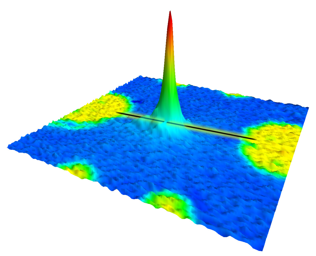
A microscope image of the light sensor shows the peaking photocurrent as it originates from the gap between the Etch A Sketch nanowires (in black). The Pitt researchers are the first to create a solid-state, oxide nanoelectronic device that combines electrical and optical capabilities onto one platform.
Topics
University Units
Media Resources
Schools of the Health Sciences Media Relations
For more information about Pitt's schools of dental medicine, health and rehabilitation sciences, medicine, nursing, pharmacy, and public health, click here >
To locate stories from health science schools prior to 2013, visit the UPMC news archives »
Urgent Question?
University of Pittsburgh news reps are available to answer urgent media inquiries. Outside of regular business hours (Mon-Fri, 8:30 a.m.-5 p.m.), please email us at media@pitt.edu.
News reps for University of Pittsburgh Health Sciences schools can be reached outside of regular business hours through the paging operator at 1+412-647-2345.